Aspherical Processing
Technology Overview
In imaging optical systems, by adding an aspherical lens as opposed to simply combining spherical lenses, it is possible to reduce aberration components that cannot be completely corrected with spherical lenses. It can also correct aberrations with a smaller number of lenses. Even in complex optical systems, design freedom is increased by using aspherical lenses and mirrors, making it possible to achieve desired design specifications.
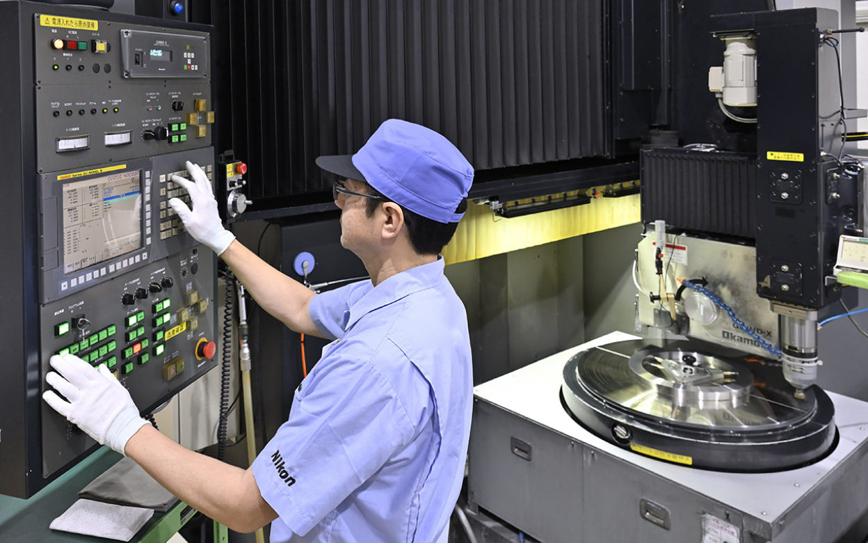
In machining, the desired shape is generally created by grinding, and the roughness of the ground surface is removed by polishing. Optical components, such as lenses, are polished to a mirror finish to prevent undesired light scattering on the surface.
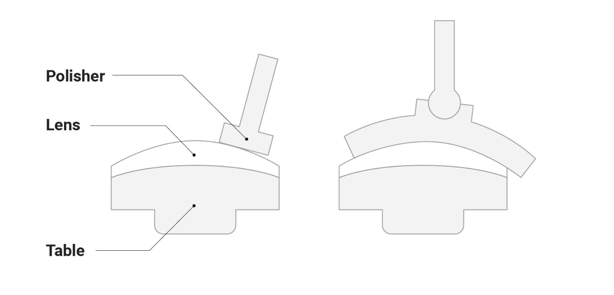
When polishing an aspherical lens, the curvature of which is not constant, it is not possible to use a method of uniformly moving a polisher with a constant curvature as when polishing spherical surfaces. Rather, a polisher smaller than the workpiece is used to polish the lens in parts while controlling the amount of polishing to create the desired shape. The amount of polishing is determined by calculating the discrepancy from the design shape based on the measurement data of the lens surface shape.
The workpiece, polisher, and abrasive must be appropriately selected. Based on these conditions, the residence time (local processing time) of the polisher on the surface is set according to the required amount of polishing.
Click to enlarge

Projection lenses for semiconductor lithography systems and other equipment must have aberrations as close to zero as possible, which requires high-precision aspherical polishing, especially for large-diameter lenses. aspherical polishing is required for materials that are difficult to shape, for lenses with large diameters, for free-form surfaces such as mirrors, and for optical parts that require high precision.
Technology Application Examples
Semiconductor Lithography Systems
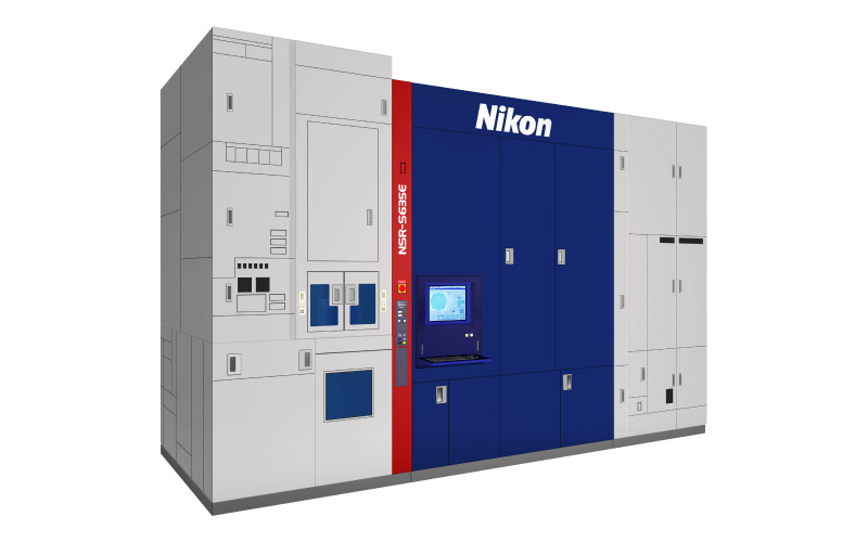
Semiconductor lithography equipment uses a projection lens that combines more than 20 lenses to expose minute electronic circuit patterns and achieve high resolution. High-precision aspherical polishing technology allows the desired imaging performance to be achieved even with a small number of lenses, making it possible to reduce weight and costs, and avoid throughput reduction by maintaining light transmission. In addition, the design freedom of optical systems such as illumination systems, increases, making it possible to control light freely.

Technologies related to these examples
Related Technology
Machining
The various parts that make up a product are primarily shaped using machine tools through processes such as cutting, grinding, and polishing. The precision of this processing affects product assembly and adjustment, and ultimately determines the product’s performance. Appropriate processing methods, jigs, and tools must be selected depending on the desired shape and the material's physical properties.
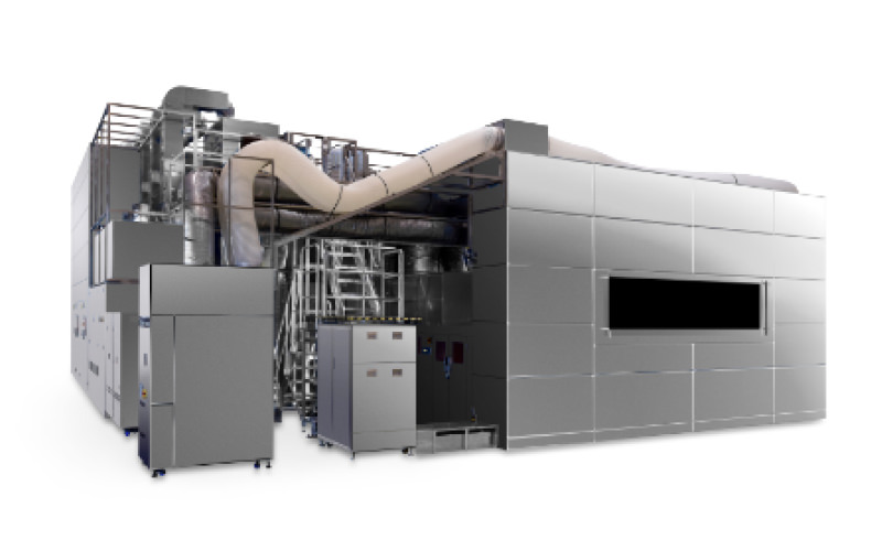
Lithography systems requires large size and high precision, so the machining of its components also requires high precision. Not only the lenses, but also the lens barrels and stages require high-precision processing. Polishing lightweight and highly rigid ceramics requires balancing physical and chemical processes to produce a highly accurate flat surface over a wide area. In order to achieve high-precision machining, high-precision measurement and machining equipment, as well as their control technology, are also required.

Main Related Products
You can search for articles related to Nikon’s technology, research and development by tag.


