Wavefront Aberration Measurement
Technology Overview
Wavefront aberration measurement is a method used to quantitatively evaluate the performance of imaging optical systems, such as camera lenses and the projection lenses of semiconductor lithography systems. Compared to other aberration measurements, it is possible to evaluate multiple types of aberration components at once, and is used when adjusting optical systems and ensuring optical performance.
A wavefront is an equiphase surface when light is treated as a wave. In an ideal imaging optical system, light emitted at one point propagates as a diverging spherical wave, which is converted into a convergent spherical wave by the imaging optical system and focused on a single point. In an actual imaging optical system, the light cannot be completely converted into a convergent spherical wave, and the imaged wavefront is slightly distorted from a spherical surface. This deviation from an ideal spherical surface is called wavefront aberration.
A typical method for measuring wavefront aberration is to measure the phase difference between two beams of lights (the wavefront aberration) by measuring the interference fringes between the light that makes up the image and the light focused to a single point. Another method is to use a Shack-Hartmann wavefront sensor.
Click to enlarge

The projection lenses used for lithography systems require highly accurate measurement of the wavefront aberration in huge optical systems. We have a variety of measurement methods to suit different situations and accuracy requirements, such as the lens assembly and adjustment process, and for correcting aberrations caused by environmental changes within the systems.
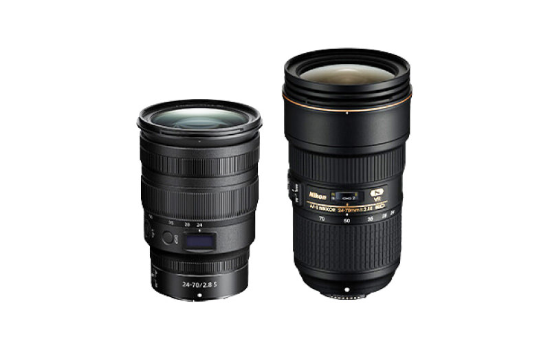
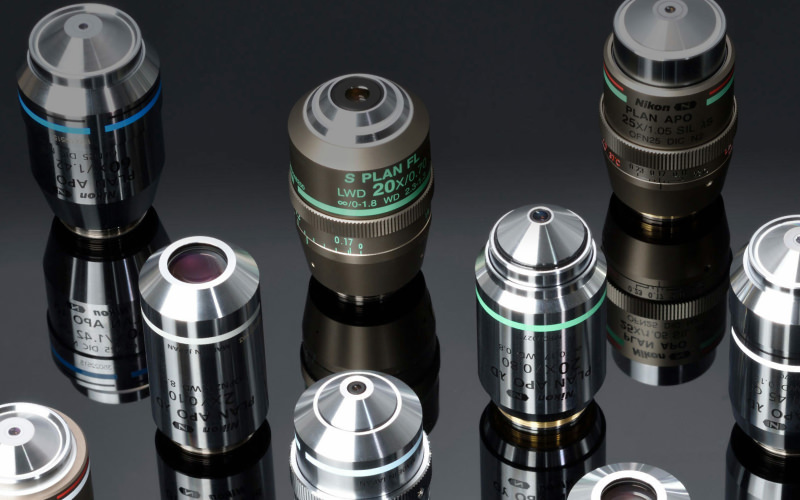
The measurement of wavefront aberration for camera lenses must accommodate various lens types with different focal lengths, such as wide-angle and telephoto lenses. In contrast, the measurement for objective lenses must be compatible with a wide wavelength band. In camera lenses, the characteristics of the remaining aberrations become the “character” of the lens, so aberrations are adjusted to produce photos suited to the target user’s preferences.
Technology Application Examples
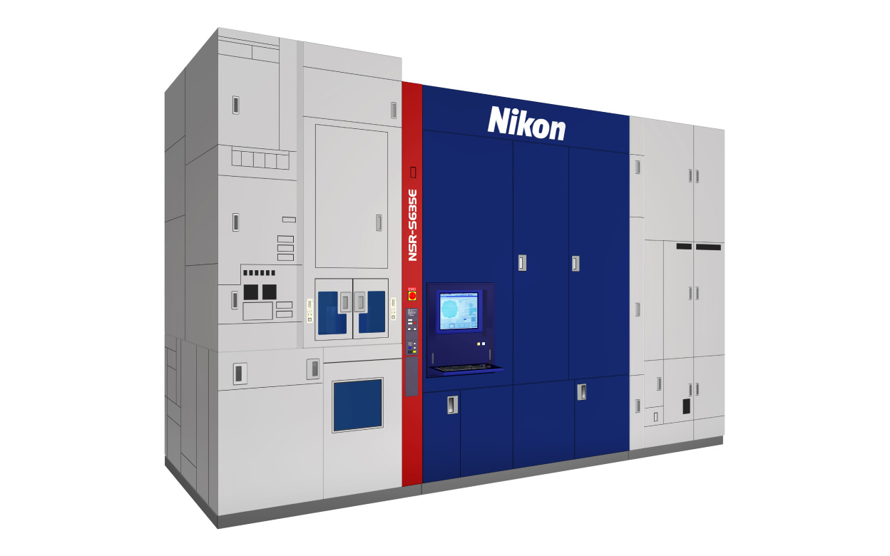
Semiconductor Lithography Systems
Semiconductor electronic circuit patterns are drawn on a large glass plate (photomask), and a lens is used to reduce and project the circuit pattern onto a silicon plate (silicon wafer) for exposure. The "semiconductor lithography system" is responsible for this process. Lenses employed for this system require the highest resolution possible with absolutely minimized aberration in order to expose fine patterns accurately. Even though a semiconductor lithography system achieves high resolution by employing high-precision lenses with the highest accuracy, aberrations can still occur in the lenses when the device is operated. This is because temperature changes occur on the lenses, which alters the refractive index. Active optics play a major role in correcting these aberrations. The pattern of aberrations that occurs during operation is very complex, and it changes constantly depending on the operating conditions and the air pressure. At Nikon, aberrations are effectively compensated by pushing and pulling the mirror that reflects the laser light as necessary with multiple actuators to slightly deform it, or by controlling the tilt of the lens.

Technologies related to these examples
Related Technology
Imaging Performance Measurement
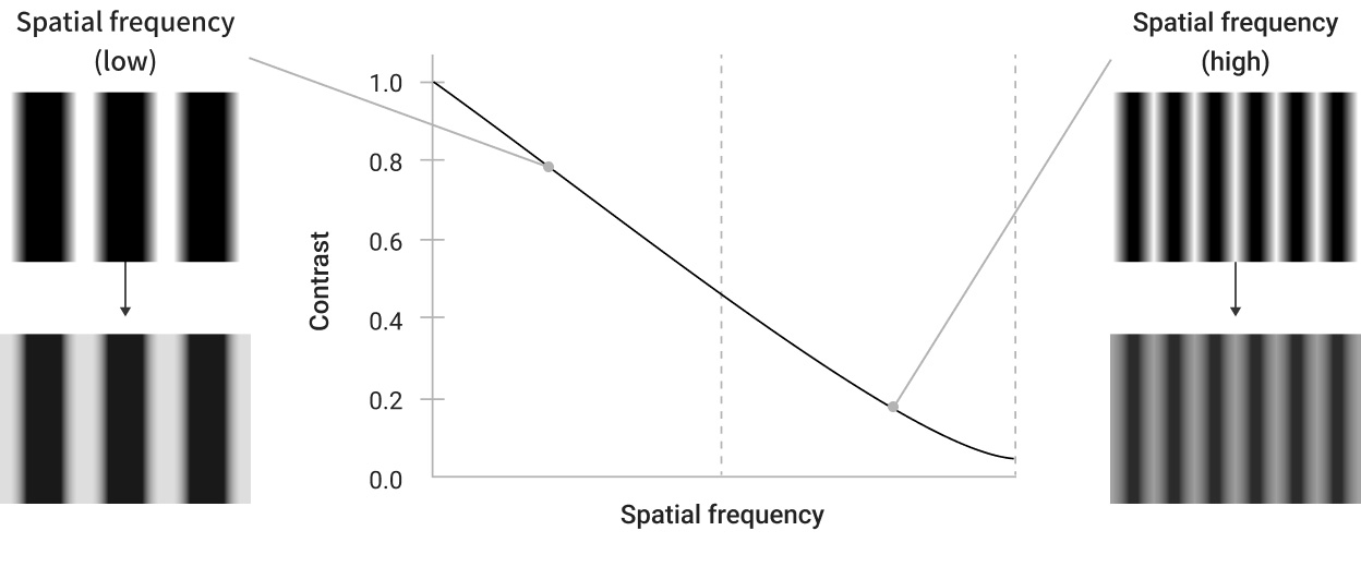
Indicators of imaging performance include not only aberration, but also the intensity distribution of point images (PSF:Point Spread Function) and the spatial frequency response (MTF: Modulation Transfer Function) of the imaging system. By measuring these, it is possible to quantitatively evaluate the performance of the imaging optical system. PSF has the advantage of being able to directly evaluate the actual image formation, and MTF measurement has the advantage of being able to evaluate image contrast.
Nikon handles imaging optical systems such as projection lenses, interchangeable camera lenses, and objective lenses, which vary in required imaging performance, optical system size, wavelength range, and production volume. In addition, measurement constraints, such as speed and simplicity, depend on the purpose, like adjustment during production or correction within the instrument, and appropriate methods are chosen based on the specific purpose and object to be measured.
Main Related Products
You can search for articles related to Nikon’s technology, research and development by tag.


