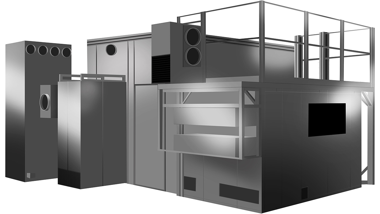
Nikon Announces Development of a Digital Lithography System with 1.0 micron (L/S*1) resolution
Nikon's first semiconductor lithography system for packaging applications
October 22, 2024

TOKYO - Nikon Corporation (Nikon) is developing a digital lithography system with resolution of one micron (L/S) and high productivity for advanced semiconductor packaging applications. This product is scheduled to be released in Nikon's fiscal year 2026.
The rapid adoption of artificial intelligence (AI) technology is driving demand for integrated circuits (ICs) for data centers. In the field of advanced packaging, including chiplets, the size of packages is increasing with the miniaturization of wiring patterns. This will lead to heightened demand for panel level packages that use glass and other materials suitable for larger packages, requiring exposure equipment that combines high resolution with a large exposure area. To meet these demands, Nikon is developing digital exposure equipment that combines the high-resolution technology of its semiconductor lithography systems, which has been cultivated over many decades, along with the excellent productivity made possible with the multi-lens technology*2 of its FPD lithography systems.
The digital lithography system does not use photomasks. Instead, it irradiates light from a source onto a spatial light modulator (SLM) that displays a circuit pattern and transfers it onto a substrate using a projection optical system. Since there is no need to design or produce photomasks, the digital lithography system also contributes to reducing costs, as well as shortening product development and manufacturing times.
Nikon will continue to contribute to advanced semiconductor manufacturing by providing lithography systems and solutions to fully satisfy our customers' goals and production requirements.
- *1Abbreviation for Line and Space. Refers to the width of the wiring and the space between adjacent wiring.
- *2Nikon's proprietary technology that exposes multiple projection lenses in an array and precisely controls them to produce the same effect as if a single giant lens were used. This enables patterning over a wider area with a single exposure.
The information is current as of the date of publication. It is subject to change without notice.
