Components Business

Contributing to the development of a variety of fields, from manufacturing processes to space exploration
Nikon contributes to the evolution of science technology, industry and society via diversified businesses that range from optical materials, optical components, the encoders used for robotics, and measurement and inspection systems, to the development of the latest technologies for space exploration, and photomask substrate production for FPDs.
Industrial Solutions Business
Providing an integrated suite of components, measurement tools, services, and solutions.
Nikon offers a wide range of one-stop solutions covering every stage from design and prototyping to integration and mass production of components/modules for light sources, and projection lenses components.
It also provides solutions that effectively meet a diverse range of market and customer needs by utilizing its core optical and precision technologies. This includes the encoders utilized as sensors in the joints of robots and machine tools to measure rotation amount or angle, along with a variety of measurement and inspection systems designed to accommodate different size, shape, and material requirements.
Optical components and optical materials
Solutions ranging from design consulting for optical components to prototyping and mass production. Nikon provides optical materials for light sources incorporated in semiconductor and FPD lithography systems that require high marginal accuracy and durability.

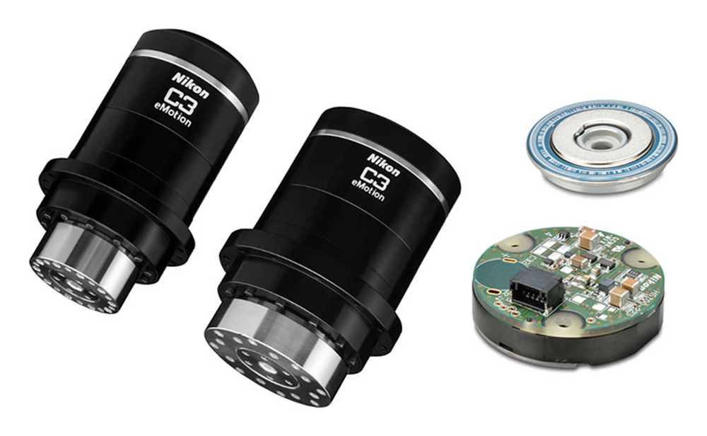
Encoders and intelligent actuator units
Measurement and control sensors are playing an increasingly important role in fields including robotics and industrial machinery. Nikon has been concentrating its unique optics, ultra-high-precision and electronics technologies on developing high-performance encoders and the intelligent actuator units for collaborative robots that incorporate them.
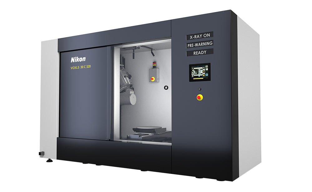
Inspection of lithium-ion batteries and castings
X-ray and CT Systems facilitate non-destructive testing, enabling measurement of objects with intricate internal structures and detection of internal defects.
Innovative in-house microfocus X-ray sources up to 450 kV achieve detailed visualization of large castings, like automotive engines, and complex samples, such as lithium-ion batteries.
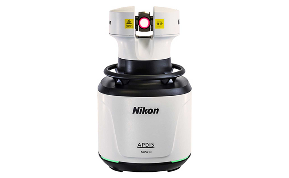
Body measurement
Laser Radar "APDIS" enables automated inspection of subjects up to 50m away. Nikon's unique technology effectively realizes the measurement of samples with various surface materials, textures, and reflectivity. In automotive manufacturing, APDIS is employed for car body and component inspection, providing instant feedback to the production process.
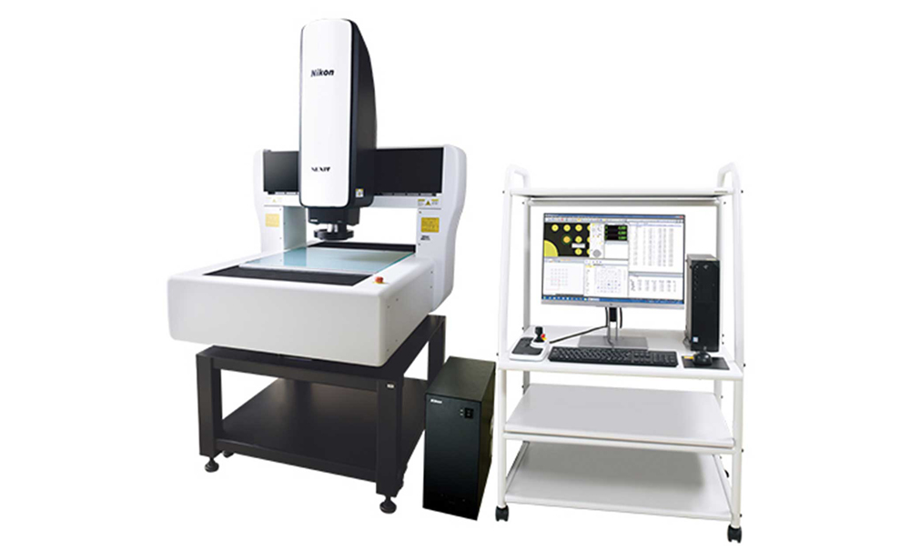
Measurement of electronic components
Digital devices, essential in modern life, as well as a variety of products across different industries and the medical field, contain many precision components. The NEXIV VMZ-S series is an image measurement system that provides non-contact, high-precision automatic measurement of the dimensions and shapes of such components.
Realizing rapid, accurate and automatic measurement of large volumes, Nikon's systems provide strong support for manufacturing sites, helping to maintain the highest quality for electronic components, semiconductors, injection-molded products, and precision machined parts.
Customized Products Business

State-of-the-art technologies for space
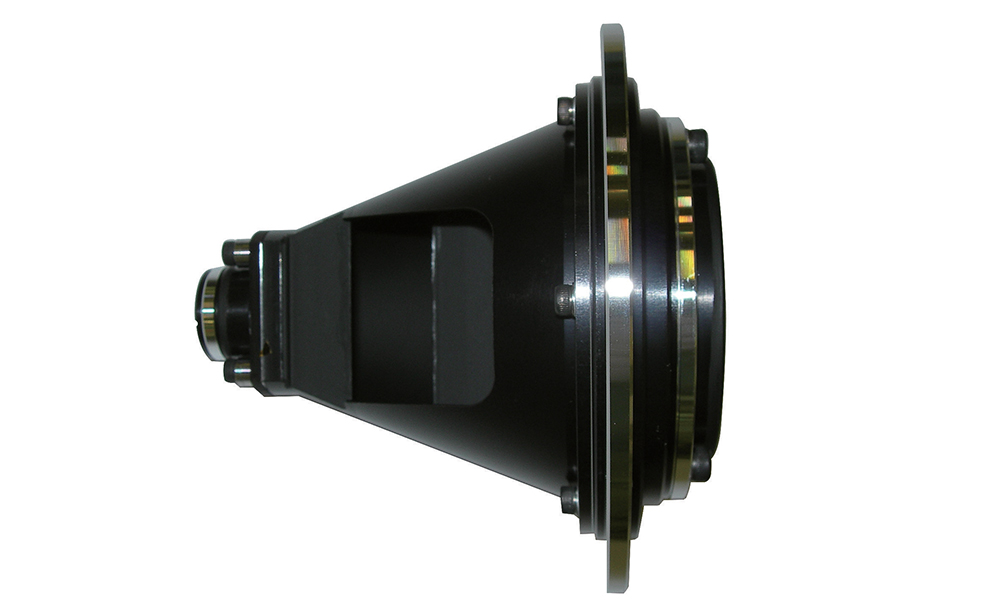
Nikon's Customized Products Business capitalizes on the company's state-of-the-art technologies to meet unique, advanced needs. Nikon handles everything from design to manufacture, providing inspection equipment for the food industry, optical products which require ultra-high precision such as those for the space and astronomical fields, including the Venus Climate Orbiter AKATSUKI and the observation systems for the Subaru large-scale optical-infrared telescope. We utilize our core technologies to the utmost to turn customers' demands into reality.
Optical systems for Akatsuki
Nikon designed and manufactured the IR1 and IR2 infrared cameras, ultraviolet imager (UVI) and lightning and airglow camera (LAC).
Glass Business

Integrated production of photomask substrates for FPD
Nikon manufactures FPD photomask substrates, which are the original patterns for electronic circuits employed in products such as LCDs, in an integrated production system that covers every step from materials to applying final processing.
Photomask substrates for FPD
Nikon uses highly transparent, highly pure materials that have superior internal qualities, such as no bubbles or inclusions. Then we produce large FPD photomask substrates as large as 2,000 mm square by utilizing precision polishing, cleaning and measurement technologies.
