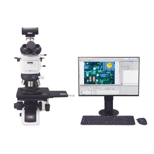
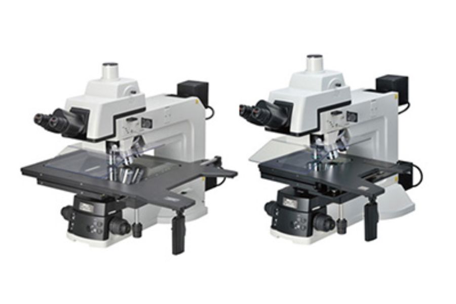
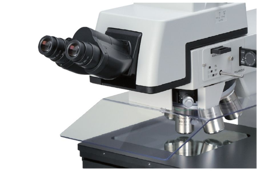
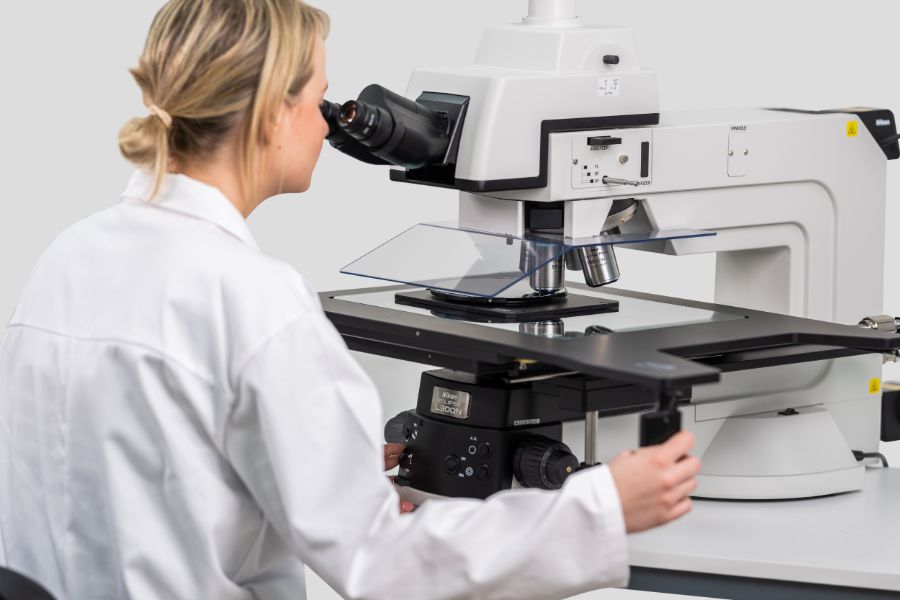
ECLIPSE L300ND, L300N and L200ND, L200N

Nikon's ECLIPSE L300ND, L300N and L200ND, L200NA is a range of semiconductor microscopes ideal for inspection of integrated circuits (IC), flat panel displays (FPD), large scale integration (LSI) electronic devices and many more applications.
ECLIPSE-L300nd-l300n-l200nd-l200n_L300Na

Advanced Semiconductor Microscopes for Inspecting the Latest Fabrications

Superb Nikon CFI60-2 optics provide excellent images to both eyepieces and also to Nikon’s digital imaging cameras with analysis software. Combining these superior optics with an extraordinary illumination system delivers images of excellent contrast and resolution.

Nikon ECLIPSE L300N(D) and L200N(D)

These microscopes are for exceptionally precise optical inspection of wafers (200mm for L200N series and 300mm for L300N series), reticules and other substrates.

Nikon CFI60-2 Optical Series

Nikon’s innovative design enables clear imaging techniques, including high contrast, brightfield, darkfield, polarisation (POL), differential interference contrast (DIC) and double beam interferometry optical contrast.

Nikon Digital Sight Cameras

The full range of Nikon’s Digital Sight cameras efficiently captures images of a sample and deliver them to the image processing software of the NIS-Elements suite, together with microscope data on the objective lens used, magnification setting and light intensity.

Integration of L200N and Wafer Loader NWL200

Nikon wafer loaders are well accepted and trusted in the semiconductor industry and many installations are in use today.

Product Highlights

Nikon CFI60-2 Optical Series

Nikon’s innovative design enables clear imaging techniques, including high-contrast, brightfield, darkfield, polarization (POL), differential interference contrast (DIC) and double beam interferometry optical contrast.

Universal Optical Contrast Methods

Reflected light: brightfield, darkfield, polarising (POL), differential interference contrast (DIC), epi-fluorescence and two-beam interferometry.
Transmitted light: brightfield, darkfield, polarising, differential interference contrast and phase contrast.

Intelligent Digital Communication

The microscope detects and controls the objective lens in use, light intensity, episcopic illumination and aperture via a USB connection to Nikon’s NIS-Elements software.

Ergonomic Design Concept

Optimal positioning of operator controls with variable angle eye-tube allows fatigue-free work.
A right-way-up, right-way-around image is provided for correctly observing raw materials, semiconductors and industrial components.

Core Features

Industries

Applications are centred around inspection duties in the electronics and telecommunications sectors.

Antennae waveguides are measured with utmost precision, as well as other components such as wafers for semiconductor or photovoltaic devices and micro electro mechanical systems (MEMS) used in smartphones, gyroscopes and accelerometers, for example.

Upright Microscopes L Series

Digital Sight Series

NIS Elements

Related Products

Software

NIS-Elements software manages Nikon Digital Sight cameras alongside Nikon microscopes to capture the best images for processing. It organises captured images and processes them logically in a smooth workflow.
Discover the Product
NWL_L200N

NWL200 Wafer Loader Series

Nikon's innovative, fully featured NWL200 wafer loaders support comprehensive inspection of 6" (150mm) and 8" (200mm) diameter semiconductor wafers by optical microscope or video measurement systems e.g. Nikon NEXIV.
Discover the Product

Speak To Us About This Product

If you would like further details on this product or a more in-depth description, our expert team will provide you with additional information and, if required, arrange an on-site visit.

Talk to us in detail about your project and our experts will advise you on the best inspection system to meet your requirements.

Please fill out the form opposite and we will get in touch with you shortly.