Ultimate resolution supported by movements as slight as 2/100,000,000,000 of a meter
Semiconductors accelerate the realization of a smart society.
Lenses used in semiconductor lithography systems that support the evolution of semiconductors require the very highest resolutions possible. One of the technologies achieving this is Nikon's cutting-edge active optics.
Advancing semiconductor lithography systems to as fine as 5 nm
A super-smart society will realize a world where anyone can comfortably live with digital devices such as smartphones. One of the key elements in creating this new society is the enhanced performance of semiconductors.
Semiconductor performance can be improved by making the width of wiring on the chip (process rule) finer and creating more complex electronic circuits.
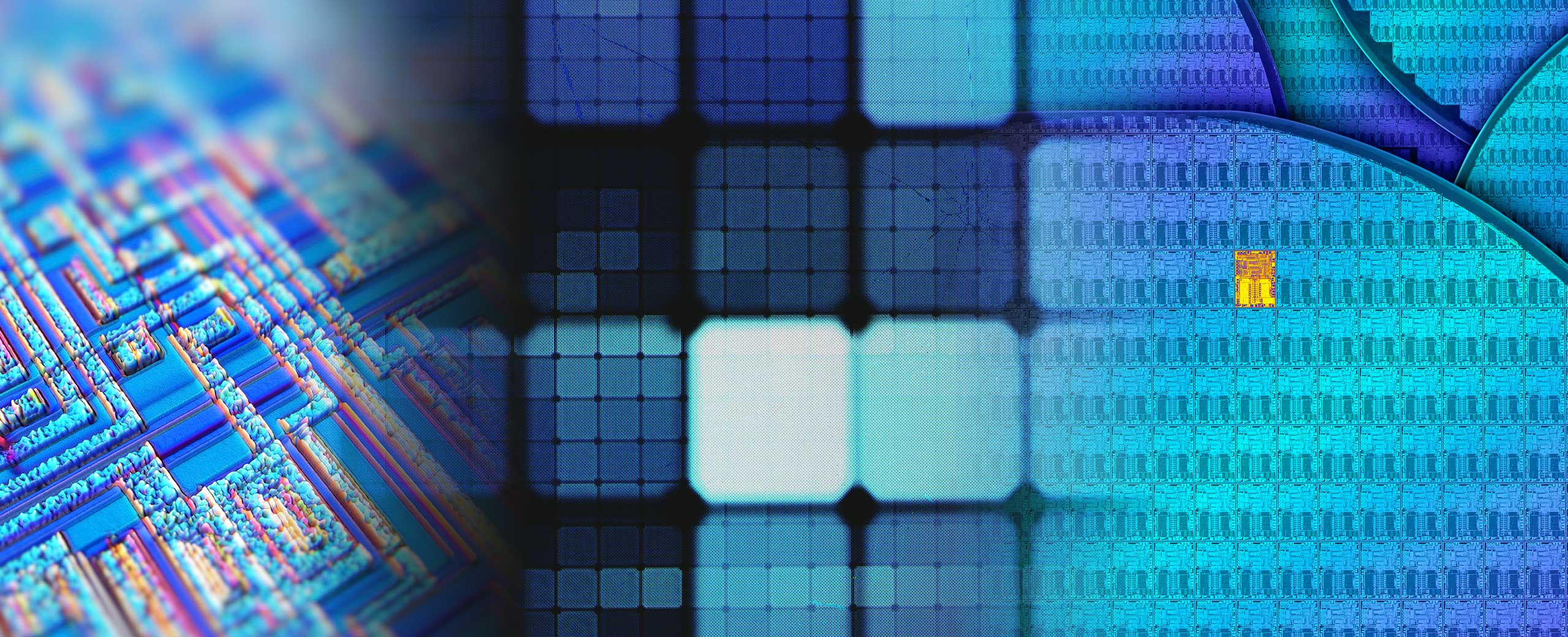
In 2018, semiconductor mass production based on the process rule of 7 nm (nanometer: 1/1,000,000,000 meters) commenced. Manufacturing based on a 5 nm process rule is also close at hand. This is equivalent to a thinness where approximately 10,000 lines could be drawn on a cross section of human hair (average thickness of 0.08 to 0.05 nm).
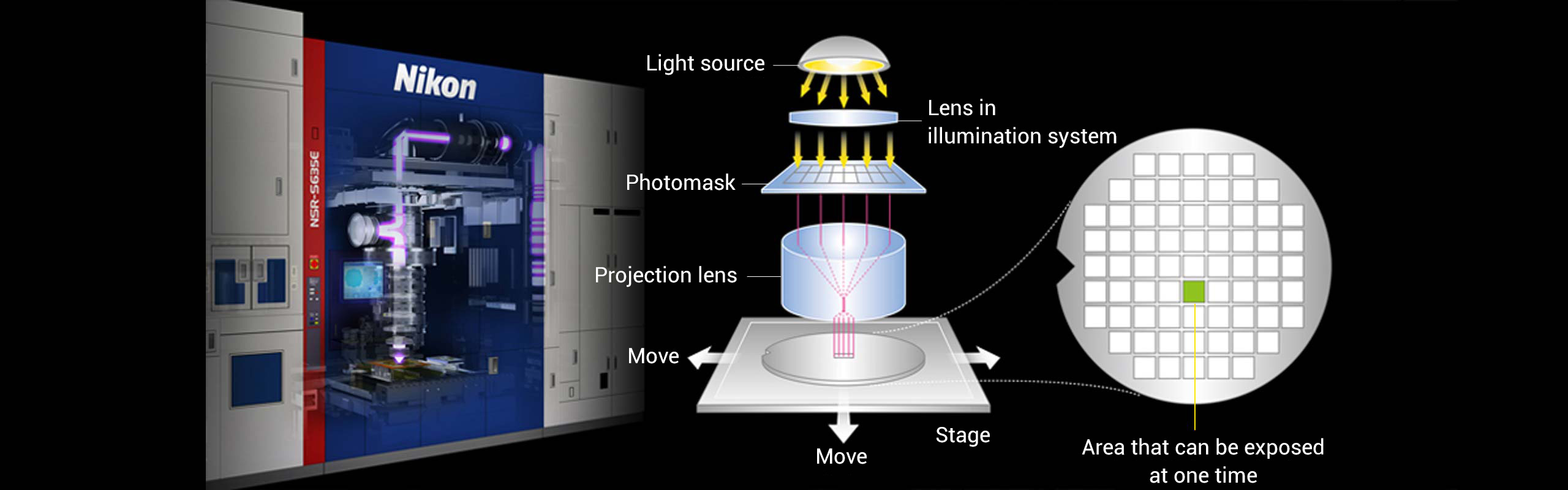
Semiconductor electronic circuit patterns are drawn on a large glass plate (photomask), and a lens is used to reduce and project the circuit pattern onto a silicon plate (silicon wafer) for exposure. The "semiconductor lithography system" is responsible for this process. Lenses employed for this system require the highest resolution possible with absolutely minimized aberration in order to expose fine patterns accurately. This lens resolution is one of the important elements that supports the evolution of semiconductors.
Resolution that can identify an object as small as 1.7 m from outer space
Let's suppose that if we were to reduce the huge area of Japan's Kanto-Koshinetsu region to the size of a postage stamp, it would be possible to identify a small car on a road on the edge of that stamp clearly, as well as at the center — the lens with the finest resolution in history, which is used in Nikon's semiconductor lithography systems is so advanced that it can project such details.

The resolution increases as lens aberrations decrease, and aberrations decrease when the lens surface is smoother. Because of this, a lens for semiconductor lithography systems is polished as smooth as possible, with surface accuracy error of only 1 nm. If these lenses' roundness was expanded to the earth's size, it would be so smooth that only 1 cm of unevenness would be observed on the ground. In addition, the lens must be installed at a specific position in the device and at a specific angle. The margin of error for this process is also at the nanometer scale.
Even though a semiconductor lithography system achieves high resolution by employing high-precision lenses with the highest accuracy, aberrations can still occur in the lenses when the device is operated. This is because temperature changes occur on the lenses, which alters the refractive index.
Active optics play a major role in correcting these aberrations.
Correcting aberrations to the limit of what is possible by deforming the reflection mirror
The pattern of aberrations that occurs during operation is very complex, and it changes constantly depending on the operating conditions and the air pressure. At Nikon, aberrations are effectively compensated by pushing and pulling the mirror that reflects the laser light as necessary with multiple actuators to slightly deform it, or by controlling the tilt of the lens.
The amount of mirror deformation is 0.02 nm (two one-hundred billionths of a meter, 2/100,000,000,000 m) at the minimum. A major advantage of this feature is that it is possible to effectively respond to aberration generation and the pattern changes. If the curved surface of the mirror was expanded to the size of the earth's surface, it would be equivalent to a slight movement of 1 mm.
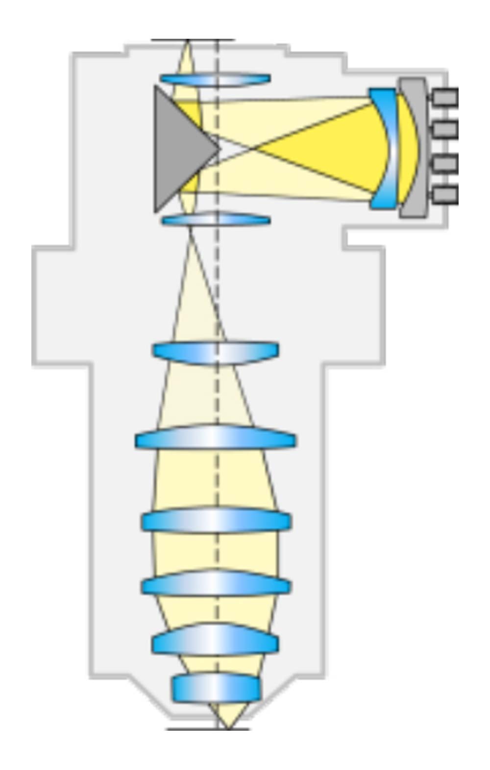
Instead of permitting laser light to pass directly through the exposure lens group, Nikon's semiconductor lithography systems employ a method that refracts laser light using a prism, reflects it with a mirror, and then returns it to the prism for passing through the lens group. By providing a deformable mirror that can control the curved surface in a complex way, high-dimensional aberration correction that cannot be achieved by just tilting the lens is effectively realized.
Furthermore, technology that corrects aberrations by heating the lens and utilizing the refractive index changes caused by temperature changes of the glass is also adopted.
The extremely high resolution of semiconductor lithography systems that supports the evolution of semiconductors is a major achievement. What makes these crucial advances possible is Nikon's unique active optics technology.
Close cooperation between development and manufacturing is the key to success
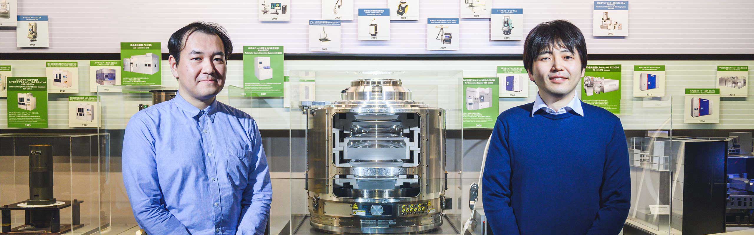
Optical Engineering Division
Hidetaka Kawahara

I am in charge of mechanical design for the lens barrel that holds the exposure lens. I was involved in this development with active optics from an early stage. For the latest models, the number of actuators has increased considerably, and the patterns to be moved have become enormous. Because of this, data cannot be processed manually, so we are developing a system from the data processing mechanism.
What I struggled with during my work on lens control was the unexpected glass deformation. I experienced it many times during development. Whenever that happened, I repeated the process of experimentation with the cooperation of the manufacturing site, taking data and investigating the cause. The cooperation and advice from the manufacturing site was extremely helpful. In the future, I would like to contribute to the development of other optical systems by utilizing my experiences with semiconductor lithography systems.
Optical Engineering Division
Yukio Koizumi

I was in charge of developing a lens controlling system that corrects aberrations via active optics. What was difficult about this was that there were problems that could not be found using simulation of the correction mechanism itself, but were discovered for the first time when they were employed for semiconductor lithography systems. At that time, we repeated discussions with the relevant departments over and over again, and eventually successfully solved every problem.
Generally, the more complex the machine, the more errors can be caused. Semiconductor lithography systems are by far the most complex, but if the system has to be halted for any reason, it can cause great losses for customers. Therefore, I think it is necessary to keep in mind that the simplest system is the best, as a designer.
- *Job title and responsibilities at time of interview.
Originally published: June 28, 2019.
Stories
- Innovating the workstyle of the livestock industry through DX
- The further development of society through semiconductors
- Rewriting the rulebook for professional cameras — A story of still shooting with the Z 9
- Pushing the limits of the photojournalism frontline — Part 2
- Pushing the limits of the photojournalism frontline — Part 1
- Manufacturing with light
- Manufacturing glass that grows like a lifeform
- Nano Crystal Coat puts innovation right before your eyes
- The compact mirrorless Z 50 packs mighty technologies
- Advancing Monodzukuri (manufacturing) through synergetic innovation
- Analyzing NIKKOR lens characteristics
- Manufacturing on a giant scale with extreme precision
- Contributing to food safety and security
- Ultimate resolution supported by movements as slight as 2/100,000,000,000 of a meter
- Revealing the mysteries of the brain
- Supporting manufacturing through highly precise, non-destructive inspection
- Next-level performance through posture analysis
- In the future, robots will work alongside you
- The future inspired by the possibilities of FPDs
- Key to practical application of regenerative medicine
- Investigating the Future of Earth from Venus